Gunn Kim(1), Young-Woo Son(1), Youngmi Cho(1), Seungwu Han(2), Hosik Lee(1),and Jisoon Ihm(1)
Motivated by the technical and economic difficulties in further miniaturizing silicon-based transistors with the present fabrication technologies, there is a strong effort to develop alternative electronic devices based on single molecules. Recently carbon nanotubes have been successfully used for nanometre-sized devices such as diodes, transistors, and random access memory cells. Such nanotube devices are usually very long compared to silicon-based transistors. J. Lee et al. reported a method for dividing a semiconductor nanotube into multiple quantum dots with lengths of about 10 nm by inserting Gd@C82 endohedral fullerenes.[1] The spatial modulation of the nanotube electronic bandgap was observed with a low-temperature scanning tunnelling microscope(STM). They observed that a bandgap of 0.5 eV is narrowed down to 0.1 eV at sites where endohedral metallofullerenes are inserted. This change in bandgap may be explained by local elastic strain and charge transfer at metallofullerene sites. This technique for fabricating an array of quantum dots could be used for nano-electronics8 and nano-optoelectronics.
We investigated the electronic structure of the fullerenes encapsulated inside semiconducting carbon nanotubes(~1.4 nm in diameter), the so-called nanopeapods, using the first-principles study.[1,2] In the C60@(17,0) peapod, the interwall separation between the nanotube and C60, is close to the van der Waals distance of graphite, implying an exothermic encapsulation. There is practically no strain on any bond in the nanotube or the fullerene. The orbital hybridization of LUMO + 1 (the state above the lowest unoccupied molecular orbital, t1g symmetry) of C60, rather than LUMO(t1u symmetry) as previously proposed, with the nanotube states explains the peak at ~1 eV in recent scanning-tunneling-spectroscopy (STS) data.[3]
On the other hand, for the C82@(17,0) peapod, the insertion is endothermic and the nanotube undergoes radial deformation around the fullerene. For the endohedral metallofullerenes(La@C82) nested in the strained nanotube, the charge transfer shifts the relative energy levels of the different states and produces a spatial modulation of the energy gap in agreement with experiment.[1]
References
[1] J. Lee et al., Nature (London) v.415, p.1005 (2002)
[2] Youngmi Cho, Seungwu Han, Gunn Kim, Hosik Lee, and Jisoon Ihm, PRL v.90, p.106402
(2003)
[3] D.J. Hornbaker et al., Science v.295, p.828 (2002)
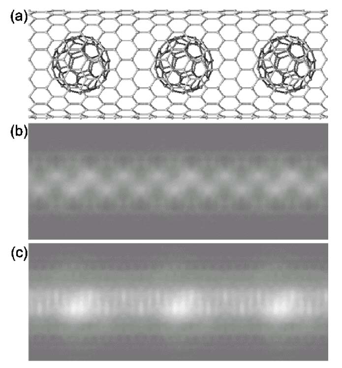
[Figure 1] Topographic STM image of C60@(17,0) peapod. (a) Model structure, (b) STM image for -1.5 V sample bias, and (c) the same image for +1.5 V sample bias.
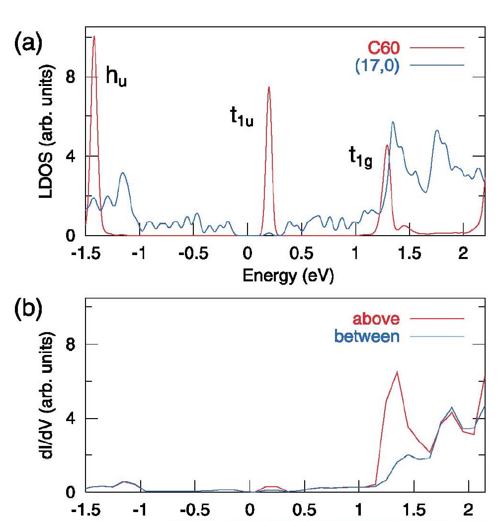
[Figure 2] (a) Local Density of the States(LDOS) of C60@(17,0), (b) Simulated dI/dV spectra of C60@(17,0) at two distinct locations, above the center of C60 (red) and between two C60's (blue).
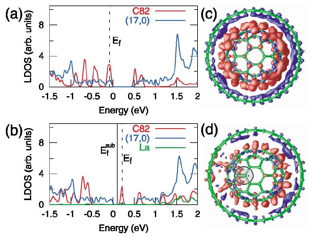
[Figure 3] Local Density of the States (LDOS) of (a) C82@(17,0) and (b)La@C82@(17,0). Isodensity surface plots are shown in (c) and (d), respectively. In figs. (c) and (d), red means electron-rich, and blue hole-rich.