Young-Woo Son, Sang Bong Lee, Chung-Ki Lee, and Jisoon Ihm
H. Kim et al. studied electronic properties of semiconductor-semiconductor(S-S) carbon nanotube junctions with different band gaps, using the scanning tunneling Microscopy(STM).[1] Characteristic features of the wave functions at different energy levels, such as a localized defect state, are clearly exhibited in the atomically resolved scanning tunneling spectroscopy(STS). According to the above experiment, the peaks of the Van Hove singularity on each side penetrate and decay into the opposite side across the junction over a distance of ~2 nm. We present the calculations on the STM images and the STS of the S-S single-walled carbon nanotube junction with different charalities, using single-electron tight-binding method. We found the following features: (1) the peaks of van Hove singularity on each side penetrate and decay slowly into the opposite side across the junction over a distance of several nanometers, (2) two localized states caused by topological defects appear in the gap of the junction, (3) the simulated STM image on the opposite side of defects also reflects the localized states, and (4) the energy of the localized state in the gap strongly depends on the number of the defects and their relative positions.
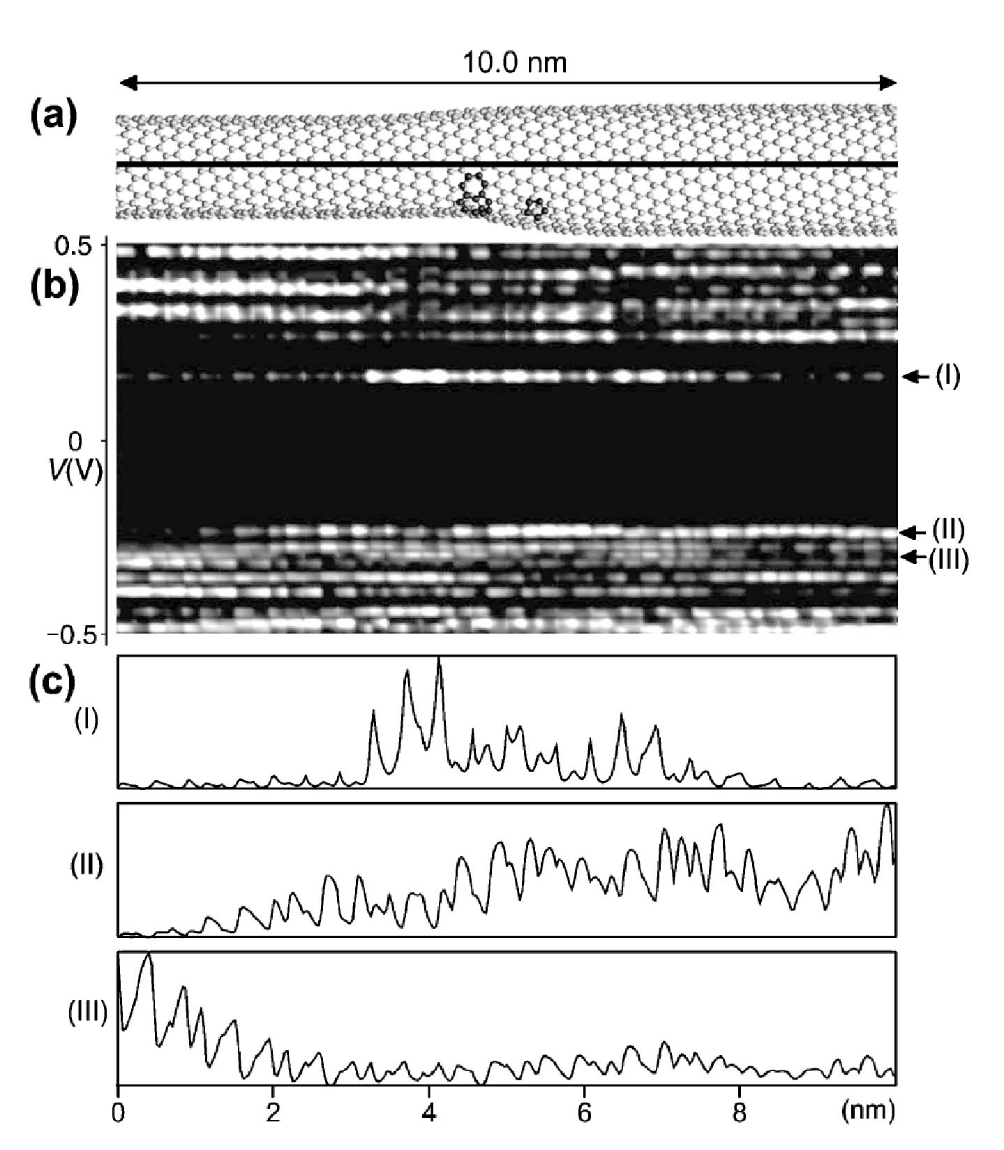
[Figure 1] Simulation of the STS on the (15,2)-(19,3) semiconducting CNT junction. (a) Model structure. The tip was scanned over the solid line in the simulation. (b) Two dimensional image of the calculated LDOS spectra. (c) The spatial distributions of the defect state above the Fermi level and the valence band edge states of both sides.
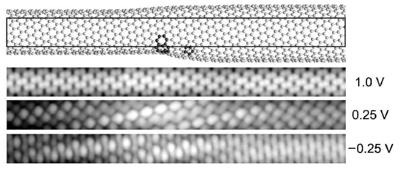
[Figure 2] Calculated topographic images of the (15,2)-(19,3) junction in the solid region at different sample bias voltage. Defects are located on the back side of the tube.