Hyoung Joon Choi(1), Young-Gui Yoon(2,3), M. S. C. Mazzoni(2,3), Steven G. Louie(2,3), Marvin L. Cohen(2,3), and Jisoon Ihm(1)
Junctions consisting of two crossed single-walled carbon nanotubes were fabricated with electrical contacts at each end of each nanotube.[1] The individual nanotubes were identified as metallic (M) or semiconducting (S), based on their two-terminal conductances; MM, MS, and SS four-terminal devices were studied. The MM and SS junctions had high conductances, on the order of 0.1 e2/h (where e is the electron charge and h is Planck's constant). For an MS junction, the semiconducting nanotube was depleted at the junction by the metallic nanotube, forming a rectifying Schottky barrier. M.S. Fuhrwe et al. used two- and three-terminal experiments to fully characterize this junction.
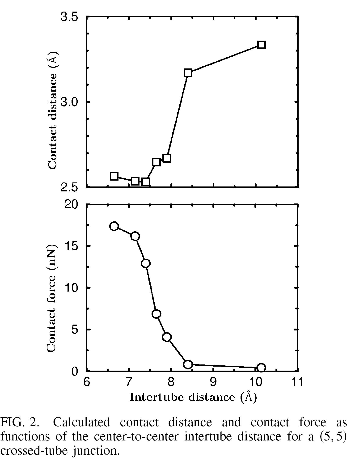
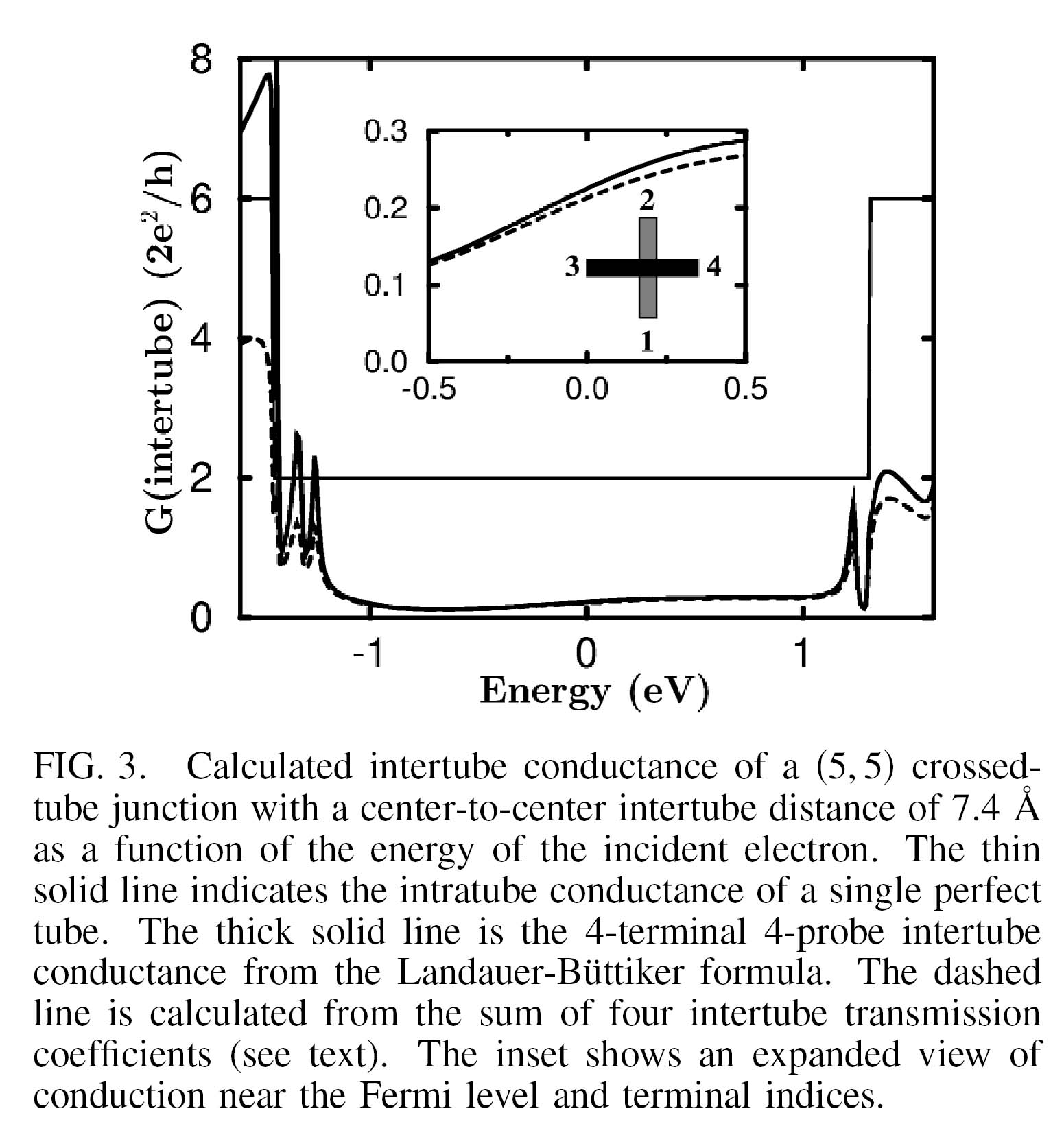
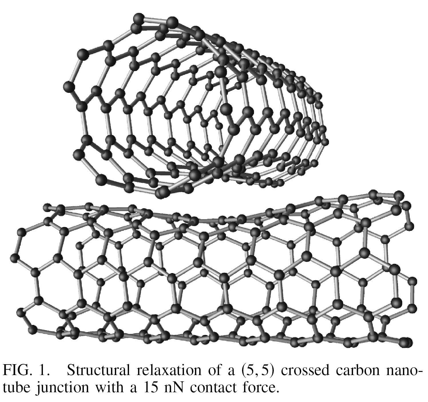
We present a first-principles study of the structure and quantum electronic conductance of junctions consisting of two crossed (5,5) single-walled carbon nanotubes.[1,2] The structures are determined by constrained minimization of total energy at a given force between the two tubes, simulating the effects of substrate-tube attraction or an applied force. We find that the intertube contact distance is very sensitive to the applied force in the range of 0-10 nN. The intertube conductance is sizable for realistic deformation expected from substrate interaction. The results explain the recent transport data on crossed nanotubes and show that these systems may be potentially useful as electromechanical devices.